Selecting the appropriate stencil thickness for your printed circuit board (PCB) assembly is a critical decision that significantly impacts the solder paste deposition process and, consequently, the overall quality and reliability of your electronic product. The stencil thickness directly influences the volume of solder paste deposited on the pads, which in turn affects the solder joint integrity. In this guide, we will delve into the considerations and factors that help you determine the optimal stencil thickness for your pcb stencil maker assembly needs.
Factors Influencing Stencil Thickness
Component Types and Sizes:
The size and type of components on your PCB play a significant role in stencil thickness selection. Smaller components with finer pitch require a thinner stencil to ensure precise solder paste deposition.
Pitch and Aperture Design:
The pitch, or distance between adjacent solder pads, dictates the spacing required between the stencil apertures. Fine-pitch components demand thinner stencils to accommodate closer apertures and maintain accurate alignment.
Solder Paste Type:
The type of solder paste you intend to use influences stencil thickness. Different pastes have varying rheological properties that can affect how they flow through apertures. Thicker pastes might necessitate slightly thicker stencils.
Production Volume:
The production volume impacts your decision as well. High-volume production might necessitate stencils with greater durability, which can be achieved with slightly thicker stencil materials.
Stencil Material:
Stencil materials, such as stainless steel or nickel, can influence the appropriate thickness. Thicker materials might be more suitable for rigorous production environments.
PCB Design and Layout:
The complexity and density of your PCB layout can also impact stencil thickness. A denser layout might require finer solder paste deposition, leading to a thinner stencil.
Choosing the Right Stencil Thickness
Standard Stencil Thicknesses:
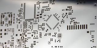
Stencil manufacturers typically offer a range of standard stencil thicknesses, such as 0.125mm (5 mils), 0.15mm (6 mils), 0.2mm (8 mils), and 0.25mm (10 mils). These options provide flexibility to match the specific requirements of your design.
Fine-Pitch Components:
For PCBs containing fine-pitch components with tight pad spacing, opt for thinner stencil thicknesses such as 0.125mm (5 mils) or 0.15mm (6 mils). These stencils enable precise paste deposition.
Medium and Coarser Pitches:
PCBs with larger components or relatively coarser pitch can utilize thicker stencil options, like 0.2mm (8 mils) or 0.25mm (10 mils). These stencils accommodate slightly larger apertures while maintaining appropriate solder paste volumes.
The pcbasic stands out as a premier SMT stencil manufacturer. Explore exclusive offers tailored to your needs for an exceptional experience.
Volume Considerations:
For high-volume production, consider a thicker stencil material for increased durability. However, ensure that the selected thickness aligns with the components’ specifications and the PCB design.
Prototyping and Custom Requirements:
In prototyping or specialized cases, custom stencil thicknesses might be required. Collaborate with your stencil manufacturer to create stencils tailored to your specific needs.
Consulting Stencil Manufacturers:
Stencil manufacturers possess expertise in stencil selection. Engage with them to discuss your design and requirements. They can provide valuable insights and recommendations based on their experience.
Impact of Stencil Thickness on Solder Paste Deposition
If the stencil is too thin for the components and design, inadequate solder paste can be deposited on the pads. This can result in insufficient solder joints, affecting connectivity and reliability.
Overly thick stencils might lead to excessive solder paste deposition, causing bridging between pads and components. This can result in short circuits and poor solder joint quality.
The stencil thickness has a direct correlation with the amount of solder paste deposited on the pads. Achieving the right balance of solder paste volume is crucial for proper solder joint formation during the reflow soldering process.
Thinner Stencils and Paste Volume:
Thinner stencils, such as 0.125mm (5 mils) or 0.15mm (6 mils), are often used for fine-pitch components. These stencils enable precise control over solder paste volume, as they allow for tighter spacing between apertures. This precise control is essential to prevent solder bridging, especially in designs with closely spaced pads.
Controlled Collapse Chip Connection (C4):
For advanced technologies like Controlled Collapse Chip Connection (C4) or ball grid array (BGA) components, which have solder balls underneath, thin stencils are preferred. These stencils ensure that the right amount of solder paste is deposited onto the solder balls, preventing excessive solder from interfering with the connection.
Thicker stencils, such as 0.2mm (8 mils) or 0.25mm (10 mils), allow for slightly larger apertures, leading to increased solder paste volume deposition. This can be advantageous for larger components or designs with coarser pitches, where a bit more solder paste is needed to create reliable solder joints.
Achieving the right solder paste volume is a balancing act. Too little solder paste can result in weak or incomplete solder joints, while too much solder paste can lead to bridging or solder ball formation.
The stencil thickness also impacts the solder paste printing process itself. The way solder paste is transferred through the stencil apertures and onto the pads is influenced by the stencil’s mechanical properties.
Thicker stencils tend to be stiffer, which can aid in maintaining alignment between the stencil and the PCB during the printing process. This is particularly useful when the PCB or the stencil is large, as it minimizes the risk of misalignment.
The thickness of the stencil affects the pressure required during the squeegee process. Thicker stencils might require slightly more pressure to ensure proper paste transfer, while thinner stencils might need gentler pressure to prevent smearing.
Printed Circuit Board Warpage:
In cases where the printed circuit board is prone to warping or bending during the printing process, a slightly thicker stencil can help compensate for the warpage by maintaining consistent pressure across the stencil.
Another consideration in stencil thickness selection is the durability of the stencil during repeated use. Thicker stencils tend to be more robust and resistant to wear and tear, making them suitable for high-volume production environments.
Thicker stencils can withstand more printing cycles without experiencing significant wear. This durability is particularly valuable in scenarios where the stencil will be used repeatedly over an extended period.
Thicker stencils are less prone to deformation, which can occur due to the pressure exerted during the squeegee process. This ensures that the stencil retains its original shape and maintains consistent aperture dimensions.
Production Environment:
In high-throughput production environments, where stencils are frequently used, thicker stencils are preferred to minimize downtime caused by stencil replacement.
Conclusion
Selecting the appropriate stencil thickness for your PCB assembly is a critical step in ensuring the reliability and quality of your electronic products. The decision involves a careful consideration of factors such as component types, pitch, solder paste type, production volume, and PCB layout. By assessing these factors and collaborating with stencil manufacturers, you can make an informed decision regarding the ideal stencil thickness. Achieving the right balance between solder paste deposition and pad alignment is essential for producing robust and functional PCB assemblies.


